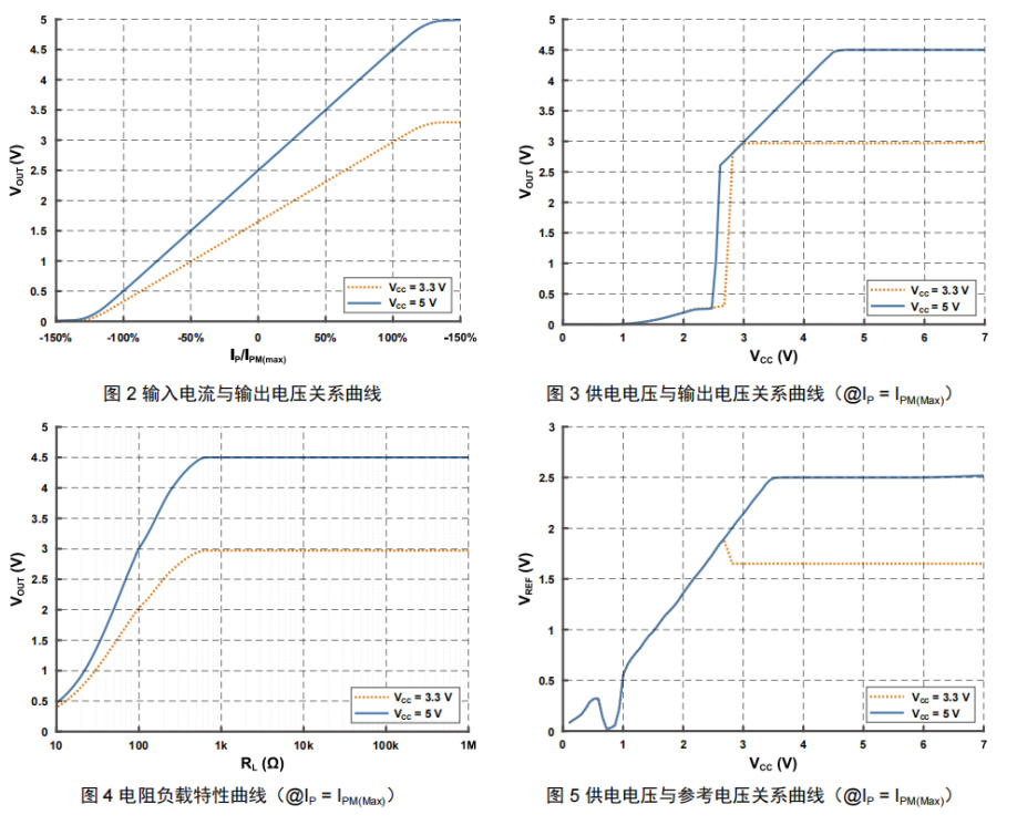
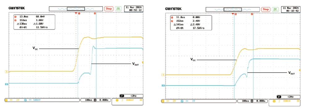
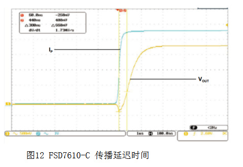
The following curves are tested according to FSD7616-050C5BFB as an example:


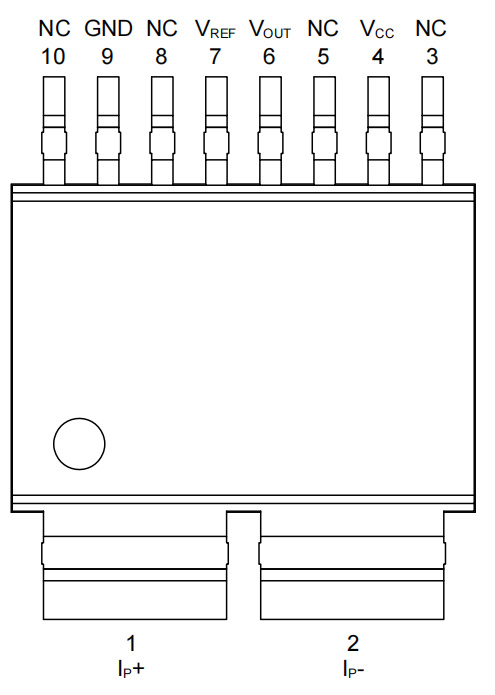
| Serial number | Pin name | Feature |
| 1 | IP+ | Current flowing in, positive direction |
| 2 | IP- | Current flowing out, negative direction |
| 3 | NC | No internal electrical connection, suspended by default |
| 4 | VCC | Power supply |
| 5 | NC | No internal electrical connection, suspended by default |
| 6 | VOUT | Analog voltage output |
| 7 | VREF | Reference voltage |
| 8 | NC | No internal electrical connection, suspended by default |
| 9 | GND | electrically |
| 10 | NC | Internal no electrical connection, default suspension Internal no electrical connection, default suspension |
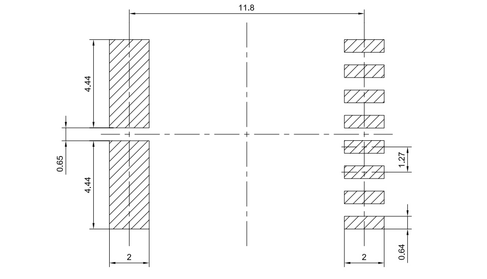
The relationship between junction temperature and primary current of FSD7610-C series chips is measured with the following experimental DEMO board.
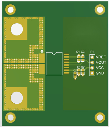
| PCB DEMO board information | |
| Number of floors | 2 layer |
| Original side path copper-covered single-layer area | 450 mm2 |
| Single layer copper coating thickness | 4Oz |
Figure 17 PCB DEMO reference layout diagram
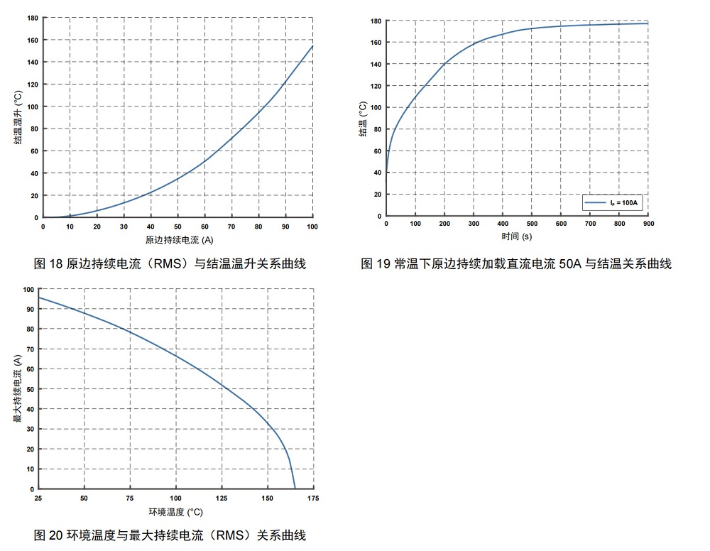
The temperature rise of the FSD7610-C junction is mainly due to the spontaneous heat of the current flowing through the path of the primary conductor, and the heat is conducted through the plastic sealing body, lead frame, PCB and air. At normal temperature, the relationship curve between continuous loading current (RMS) of FSD7610-C and junction temperature rise increment is shown in Figure 18. In the environment of natural air flow at normal temperature, the junction temperature of FSD7610-C generally tends to be stable when the continuous current is loaded for about 10min. As shown in Figure 19, when the DC current is continuously loaded for 100A at 26°C, the relationship between the junction temperature rise and the loading current time is about 350s. The chip junction temperature is close to 165°C.
The relationship curve between the maximum continuous current loading capability (current RMS) of FSD7610-C and operating ambient temperature is shown in Figure 20. When the ambient temperature is 25°C, the maximum continuous current RMS is 96A. At 125 degrees, that about 54A. If the junction temperature does not exceed 165°C, the surge or pulse current is allowed to exceed the maximum value listed in the diagram.
Instructions
1)Incorrect cables may damage the sensor.
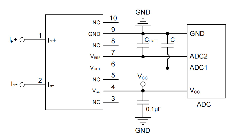
2) The product power supply voltage VCC must meet specifications. If the voltage is too low, the product cannot be accurately output. If the voltage is too high, the product may be damaged.
3) The RC filtering link between product output VOUT and GND can be added according to actual requirements to adjust product output frequency characteristics.
4) Sensors can be customized according to customer requirements, including supply voltage, measurement current range, pin definition, and more.
• 10-pin SOPW package
• High precision
• Low noise
• Wide frequency band, fast response
• Excellent temperature stability
• RoHS & REACH compliant
• Inverter current detection
• Power monitoring
• Motor drive
• Photovoltaic inverter
• Overcurrent protection
Parameter | Symbol | Minimum value | Maximum value | Unit |
Supply voltage | VCC | - | 6 | V |
ESD Performance (HBM) | VESD | - | 4 | kV |
Service temperature | TA | -40 | 125 | °C |
Storage temperature | TSTG | -40 | 125 | °C |
Maximum junction temperature | TJ(MAX) | - | 165 | °C |
Parameter | Symbol | Rated value | Unit |
Compressive strength of insulation | VD | 4.8 | kV(50Hz, 1min) |
Maximum operating isolation voltage | VISO | 1618 | VPK |
1144 | VRMS | ||
Creepage distance | dCP | 8.2 | mm |
Electrical clearance | dCL | 8.2 | mm |
Relative leakage marking index | CTI | ≥ 600 | V |
Parameter | Symbol | Conditions | Minimum value | Typical value | Maximum value | unit |
Supply voltage | VCC | FSD7610-XXXC3BFB | 3 | 3.3 | 3.6 | V |
FSD7610-XXXC5BFB | 4.5 | 5 | 5.5 | |||
Zero bias voltage | VOFF | IP = 0, VCC = 3.3 V,FSD7610-XXXC3BFB | - | 1.65 | - | V |
IP = 0, VCC = 5 V,FSD7610-XXXC5BFB | - | 2.5 | - | |||
Output saturation voltage | VOL | - | 0.2 | - | - | V |
VOH | - | - | - | VCC - 0.2 | ||
Current consumption | IC | VCC = 3.3 V | - | - | 6 | mA |
VCC = 5 V | - | - | 6 | |||
Power-on time | tON | Stable level from VCC ≥ 2.5V to VOUT | - | 200 | - | μs |
Primary side conductor resistance | RIN | TA = 25°C | - | 0.27 | - | mΩ |
Output resistance load | RL | Between VOUT and GND | 1 | 10 | - | kΩ |
Output capacitance load | CL | Between VOUT and GND | - | - | 10 | nF |
Output pull current | IOUT(SOURCE) | VCC = 3.3V, VOUT shorted to GND | - | 43 | - | mA |
VCC = 5 V, VOUT shorted to GND | - | 45 | - | |||
Output filling current | IOUT(SINK) | VCC = 3.3V, VOUT shorted to VCC | - | 43 | - | mA |
VCC = 5 V, VOUT shorted to VCC | - | 45 | - | |||
VREF resistance load | RLREF | Between VREF and GND | 10 | 100 | - | kΩ |
VREF capacitive load | CLREF | Between VREF and GND | - | 1 | 10 | nF |
VREF pull current | IREF(SOURCE) | VCC = 3.3V, VREF short-circuited to GND | - | 3.7 | - | mA |
VCC = 5 V, VREF short-circuited to GND | - | 8.7 | - | |||
VREF perfusion current | IREF(SINK) | VCC = 3.3V, VREF short circuit to VCC | - | 0.125 | - | mA |
VCC = 5 V, VREF short circuit to VCC | - | 0.135 | - | |||
Power supply rejection ratio | PSRR | DC~1kHz, 100mV pk-pk ripple aroud VCC = 5 V, IP = 0 | - | -40 | - | dB |
Common-mode magnetic field rejection ratio | CMFRR | Uniform external magnetic field | - | -40 | - | dB |
Rise time | trise | 10% to 90% of the time from the final VOUT | - | 1.1 | - | μs |
Delay time | tD | 20% time from the final IP to the corresponding VOUT | - | 0.4 | - | μs |
Response time | tR | 90% of the time from the final IP to the corresponding VOUT | - | 1.2 | - | μs |
bandwidth | BW | IP = 10A, amplitude attenuation to -3dB | - | 350 | - | kHz |
TA = 25 °C, VCC = 3.3V, RL = 10 kΩ unless otherwise specified
Parameter | Symbol | Conditions | Minimum value | Typical value | Maximum value | Unit |
Measuring range | IPM | FSD7610-050C3BFB | -50 | - | 50 | A |
FSD7610-075C3BFB | -75 | - | 75 | |||
FSD7610-100C3BFB | -100 | - | 100 | |||
FSD7610-150C3BFB | -150 | - | 150 | |||
FSD7610-200C3BFB | -200 | - | 200 | |||
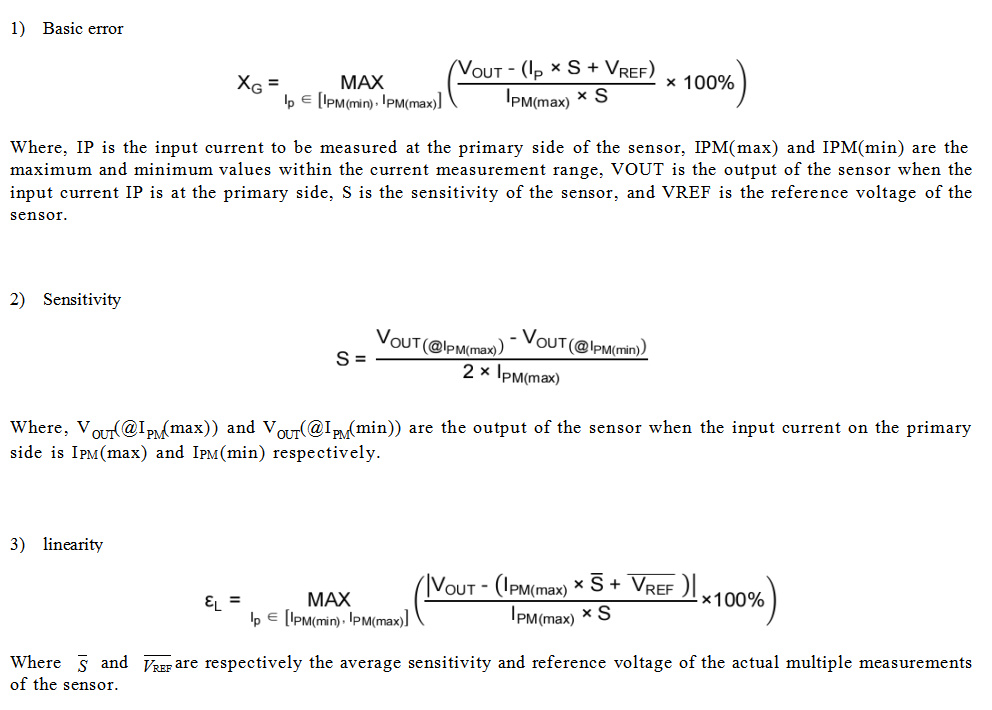
Sensitivity | S | FSD7610-050C3BFB | - | 26.4 | - | mV/A |
FSD7610-075C3BFB | - | 17.6 | - | |||
FSD7610-100C3BFB | - | 13.2 | - | |||
FSD7610-150C3BFB | - | 8.8 | - | |||
FSD7610-200C3BFB | - | 6.6 | - | |||
Basic error | XG | TA = 25 °C, IP = IPM(min) ~ IPM(max) | - | ±1 | - | %IPM(max) |
TA = -40 °C ~ +25 °C, IP = IPM(min) ~ IPM(max) | -2 | - | 2 | |||
TA = 25 °C ~ +125 °C, IP = IPM(min) ~ IPM(max) | -3 | - | 3 | |||
Linearity error | εL | IP = IPM(min) ~ IPM(max) | - | 0.5 | 1 | %IPM(max) |
Sensitivity error | εS | TA = 25 °C, IP = IPM(min) ~ IPM(max) | -1 | - | 1 | % |
TA = -40 °C ~ +25 °C, IP = IPM(min) ~ IPM(max) | -1.5 | - | 1.5 | |||
TA = 25 °C ~ +125 °C, IP = IPM(min) ~ IPM(max) | -2 | - | 2 | |||
Reference voltage | VREF | TA = 25 °C | 1.645 | - | 1.655 | V |
TA = -40 °C ~ +125 °C | 1.635 | - | 1.665 | |||
Zero offset voltage | VOE | TA = 25 °C, IP = 0, VOUT - VREF | -10 | - | 10 | mV |
TA = -40 °C ~ +25 °C, IP = 0, VOUT - VREF | -12 | - | 12 | |||
TA = 25 °C ~ +125 °C, IP = 0, VOUT - VREF | -20 | - | 20 | |||
hysteresis | VOH | IP = IPM(min) or IPM(max) → 0 | -10 | - | 10 | mV |
noise | VN | TA = 25 °C, BW = 100 kHz | - | 10 | - | mVPP |
TA = 25 °C, VCC = 5 V, RL = 10 kΩ unless otherwise specified
Parameter | Symbol | Conditions | Minimum value | Minimum value | Minimum value | Unit |
Measuring range | IPM | FSD7610-050C5BFB | -50 | - | 50 | A |
FSD7610-075C5BFB | -75 | - | 75 | |||
FSD7610-100C5BFB | -100 | - | 100 | |||
FSD7610-150C5BFB | -150 | - | 150 | |||
FSD7610-200C5BFB | -200 | - | 200 | |||
Sensitivity | S | FSD7610-050C5BFB | - | 40 | - | mV/A |
FSD7610-075C5BFB | - | 26.67 | - | |||
FSD7610-100C5BFB | - | 20 | - | |||
FSD7610-150C5BFB | - | 13.33 | - | |||
FSD7610-200C5BFB | - | 10 | - | |||
Basic error | XG | TA = 25 °C, IP = IPM(min) ~ IPM(max) | - | ±1 | - | %IPM(max) |
TA = -40 °C ~ +25 °C, IP = IPM(min) ~ IPM(max) | -2 | - | 2 | |||
TA = 25 °C ~ +125 °C, IP = IPM(min) ~ IPM(max) | -3 | - | 3 | |||
Linearity error | εL | IP = IPM(min) ~ IPM(max) | - | 0.5 | 1 | %IPM(max) |
Sensitivity error | εS | TA = 25 °C, IP = IPM(min) ~ IPM(max) | -1 | - | 1 | % |
TA = -40 °C ~ +25 °C, IP = IPM(min) ~ IPM(max) | -1.5 | - | 1.5 | |||
TA = 25 °C ~ +125 °C, IP = IPM(min) ~ IPM(max) | -2 | - | 2 | |||
Reference voltage | VREF | TA = 25 °C | 2.495 | - | 2.505 | V |
TA = -40 °C ~ +125 °C | 2.48 | - | 2.52 | |||
Zero offset voltage | VOE | TA = 25 °C, IP = 0, VOUT - VREF | -10 | - | 10 | mV |
TA = -40 °C ~ +25 °C, IP = 0, VOUT - VREF | -15 | - | 15 | |||
TA = 25 °C ~ +125 °C, IP = 0, VOUT - VREF | -20 | - | 20 | |||
hysteresis | VOH | IP = IPM(min) or IPM(max) → 0 | -10 | - | 10 | mV |
noise | VN | TA = 25 °C, BW = 100 kHz | - | 10 | - | mVPP |
Type | Supply voltage | Measuring range | Zero bias voltage | sensitivity |
FSD7610-050C3BFB | 3.3 V | ±50 A | 1.65 V | 26.4mV/A |
FSD7610-075C3BFB | 3.3 V | ±75 A | 1.65 V | 17.6mV/A |
FSD7610-100C3BFB | 3.3 V | ±100A | 1.65 V | 13.2 mV/A |
FSD7610-150C3BFB | 3.3 V | ±150 A | 1.65 V | 8.8mV/A |
FSD7610-200C3BFB | 3.3 V | ±200A | 1.65 V | 6.6mV/A |
FSD7610-050C5BFB | 5 V | ±50 A | 2.5 V | 40 mV/A |
FSD7610-075C5BFB | 5 V | ±75 A | 2.5 V | 26.67 mV/A |
FSD7610-100C5BFB | 5 V | ±100 A | 2.5 V | 20 mV/A |
FSD7610-150C5BFB | 5 V | ±150A | 2.5 V | 13.33 mV/A |
FSD7610-200C5BFB | 5 V | ±200A | 2.5 V | 10 mV/A |
| Classify | Title | Download |
|---|
Leave your contacts and our engineers will help you to find the solution you are looking for.

Hi! Welcome back.
How are you doing?
Let’s talk! We’ll provide the perfect solution for you!

Shanghai Freesor Sensor Technology Co. ,Ltd. was founded in 2005 by a number of overseas returnees with rich experience. It is a high-tech enterprise integrating design, research and development, production and sales.
Sales Center Add: Room 1405-1, Building B, 333 Haiyang 1st Road, Pudong New Area, Shanghai
Factory Add:Building 4, Keland Smart Energy Industrial Park, Guangming District, Shenzhen, Guangdong Province, China.