产品特性/Product characteristics
• SOP8 封装/SOP8 package
• 精度高/High precision
• 低噪声/Low noise
• 频带宽,响应快/Wide frequency band, fast response
• 优秀的温度稳定性/Excellent temperature stability
应用领域/Applications
• 变频器电流检测/Inverter current detection
• 电源监控/Power monitoring
• 电机驱动/Motor drive
• 光伏逆变器/Photovoltaic inverter
• 过流保护/Overcurrent protection
电气参数/Electrical parameter
参数 Parameter | 符号 Symbol | 条件 Conditions | 最小值 Minimum value | 典型值 Typical value | 最大值 Maximum value | 单位 Unit |
供电电压 Supply voltage | VCC | - | 4.75 | 5 | 5.25 | V |
零点偏置电压 Zero bias voltage | VOFF | IP = 0 | - | 2.5 | - | V |
输出饱和电压 Output saturation voltage | VOL | - | 0.2 | - | - | V |
VOH | - | - | - | VCC-0.2 | V | |
电流消耗 Current consumption | IC | IP = 0 | - | 3.5 | 4 | mA |
上电时间 Power-on time | tPO | VCC ≥ 2.5V | - | 100 | - | μs |
原边导体电阻 Primary side conductor resistance | RIN | TA = 25°C | - | 1 | - | mΩ |
输出内阻 Output internal resistance | ROUT | - | - | 2 | 5 | Ω |
输出电阻负载 Output resistance load | RL | VOUT 与 GND 之间 Between VOUT and GND | - | 10 | - | kΩ |
输出电容负载 Output capacitance load | CL | VOUT 与 GND 之间 Between VOUT and GND | - | - | 10 | nF |
输出拉电流 Output pull current | IOUT(SOURCE) | VOUT 短路到 GND VOUT shorted to GND | - | 85 | - | mA |
输出灌电流 Output filling current | IOUT(SINK) | VOUT 短路到 VCC VOUT shorted to VCC | - | 65 | - | mA |
VREF 电阻负载 VREF resistance load | RLREF | VREF 与 GND 之间 Between VREF and GND | - | 10 | - | kΩ |
VREF 电容负载 VREF capacitive load | CLREF | VREF 与 GND 之间 Between VREF and GND | - | - | 100 | pF |
上升时间 Rise time | trise | IP = 20 A(100 A/μs) | - | 0.5 | - | μs |
延迟时间 Delay time | tD | IP = 20 A(100 A/μs) | - | 0.3 | - | μs |
响应时间 Response time | tR | IP = 20 A(100 A/μs) | - | 0.5 | - | μs |
带宽 bandwidth | BW | 小信号 -3dB Small signal -3dB | - | 500 | - | kHz |
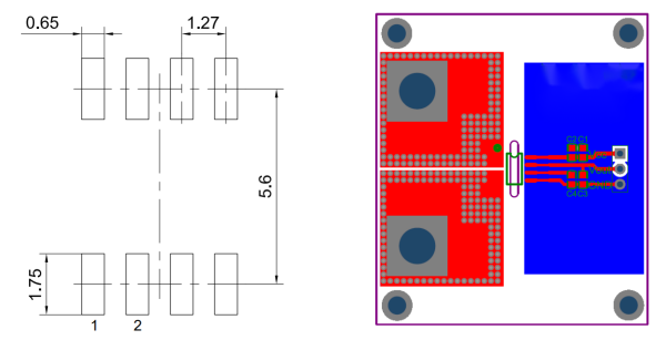
PCB 推荐布局/PCB recommended layout

FSD7608-C 在大电流量程应用中,由于电流流经原边路径会产生一定的热量,采用合适的Layout,比 如增加铺铜厚度、面积以及 PCB 层数,可以有更好的散热效果。FSD7608-C 芯片底部 PCB 开槽,可以增加 爬电距离。
FSD7608-C in the application of large current range, because the current flows through the original side path will produce a certain amount of heat, the use of appropriate Layout, such as increasing the thickness of copper, area and the number of PCB layers, can have a better heat dissipation effect. FSD7608-C chip bottom PCB slot, can increase the creepage distance.
使用说明/Instructions
1) 错误接线可能导致传感器损坏。
Incorrect cables may damage the sensor.
2) 产品供电电压 VCC需要满足规格要求,过低会导致产品无法准确输出,过高则会导致产品损坏。
The product power supply voltage VCC must meet specifications. If the voltage is too low, the product cannot be accurately output. If the voltage is too high, the product may be damaged.
3) 产品输出 VOUT 与 GND 之间可根据实际需求增设 RC 滤波环节,以调整产品输出频率特性。
The RC filtering link between product output VOUT and GND can be added according to actual requirements to adjust product output frequency characteristics.
4) 可根据客户需求定制传感器,包括供电电压、测量电流范围、引脚定义等。
Sensors can be customized according to customer requirements, including supply voltage, measurement current range, pin definition, and more.
| Classify | Title | Download |
|---|
Leave your contacts and our engineers will help you to find the solution you are looking for.

Hi! Welcome back.
How are you doing?
Let’s talk! We’ll provide the perfect solution for you!

Shanghai Freesor Sensor Technology Co. ,Ltd. was founded in 2005 by a number of overseas returnees with rich experience. It is a high-tech enterprise integrating design, research and development, production and sales.
Sales Center Add: Room 1405-1, Building B, 333 Haiyang 1st Road, Pudong New Area, Shanghai
Factory Add:Building 4, Keland Smart Energy Industrial Park, Guangming District, Shenzhen, Guangdong Province, China.